EE4449 Logic Design and Logic Synthesis Lab 1
Lab 1 for EE4449 Logic Design/Logic Synthesis Course at HCMUT
LAB 1 - EE4449 - HCMUT
Warmup
Objective and Overview
The purpose of this project is to brush off any dust that has accumulated on your SystemVerilog skills. It’s as much about getting an FPGA programming environment set up as anything else. As such, this project is significantly simpler than any other course project; and, therefore, worth far fewer points.
This is an group project, to be done in simulation with MODELSIM/QUESTASIM OR VSIM and on Quartus for your Altera DE10 board. Please tick on optimization with full visibility on QuestaSim.
A Note about Collaboration
Project 1 is to be accomplished in a group. All work must be your own.
Hints from others can be of great help, both to the hinter and the hintee. Thus, discussions and hints about the assignment are encouraged. However, the project must be coded and written up in a group (you may not show, nor view, any source code from other students). We may use automated tools to detect copying.
Use Emails/LMS to ask questions or come visit us (203B3) during office hours.
We want to see you succeed, but you have to ask for help.
Background
Over the semester we’ll do several assignments (homeworks and/or projects) that are to be implemented and demonstrated on the Altera DE10 boards at the lab. The kit you’ll use contains the board, power supply, and a USB A to USB B cable.
The basic idea here is to install the software on your computer, run it to develop the system described here, and turn your code in, all before the due date.
The software is available for Windows and Linux. Install it from the DVD or download it at http://fpgasoftware.intel.com. The latest version of Quartus will work, but remember to install the Cyclone V library when prompted.
If you have a Mac (lucky you), you will have to use a virtual machine (Parallels, VMware, etc).
People will probably need to do something with the USB Blaster windows driver (if you have never used the kit before), which is available at: http://www.terasic.com.tw/wiki/Altera_USB_Blaster_Driver_Installation_Instructions.
Assignment Overview
The repo contains sumitup.sv your starter code. Also in the same repo are p1hwtb.svp. a hardware testbench, and p1simtb.sv as simulation testbench. DE10_Standard_Pin_Assignment.qsf is a pin definition file for your board. The other files are headers so that you can write the module a bit easier for both of us (DO NOT CHANGE THE HEADERS).
The basic idea of the sumitup module is to add up a series of numbers provided at its input. It is not complex at all. The go_l signal indicates when the first value is on the input. At each clock edge another value appears on the input. However, when there’s a zero on the inA input, that’s the last value and done should immediately be asserted. The sumitup module is completely and correctly specified in the sumitup.sv file you downloaded. You will not need to make any changes to the sumitup module. Obviously, there must be more to this project, then.
Your main task is to write a downstream module that captures the calculated sum and holds it for display while the next sum is being calculated. All it does is wait for the done signal and then loads the calculated sum into its own register. The captured value is then displayed on the two hex displays.
The hardware testbench, which we provide, will generate a set of random values and send them to your sumitup module (assuming you’ve wired everything together correctly). When it’s done, it displays what it thinks is the 8-bit sum of the series of values in HEX3 and HEX2 (the leftmost digits). Your sum should be displayed in HEX1 and HEX0. The idea is that if you’ve interfaced and wired everything together correctly, then the same two 2-digit hex numbers are shown in the topmost (left) and bottommost (right) hex displays. Also, in that case, the testbench will provide a signal (that you’ll hook to LEDR0) such that the LED will light up when the values match. You’ll need some combinational logic to drive the displays. (Hint: write a bcdtohex module to connect with it)
Lastly, write the p1 module to be the top module of your design, connecting everything and synthesize on Quartus. The topology should be similar to the picture below.
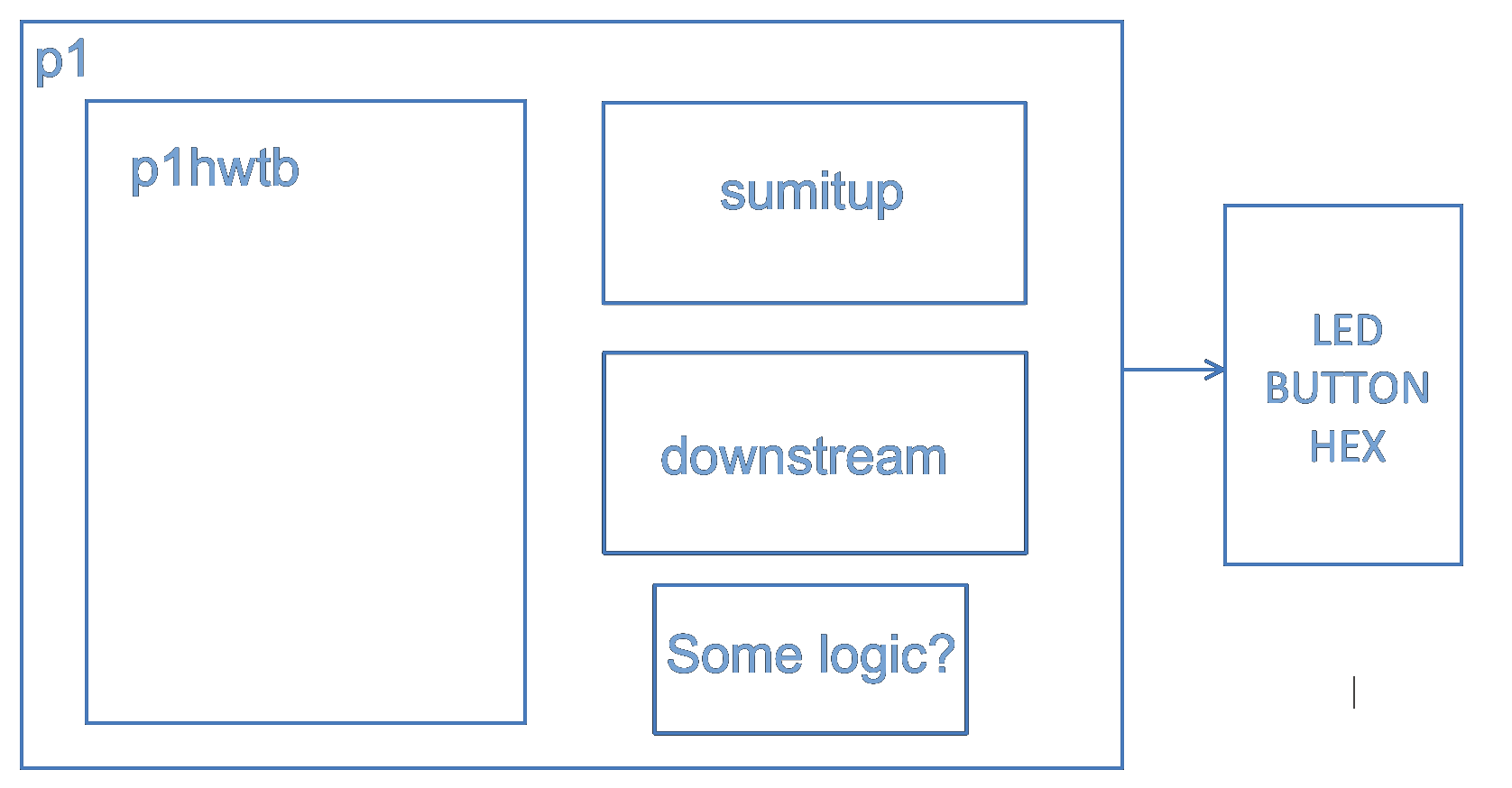 Figure 1: Topology of the design
Just to make sure you’ve thought this through, let me ask a few questions.
Are you responsible for connecting p1swtb to anything?
Your downstream module’s output value will be connected to outResult, as noted in the comments above. Should it be connected to anything else?
Does the p1hwtb testbench handle the LEDR0 connection, or do you have to do that?
If you are unsure about any of these answers, come talk to us before you start hacking away. Also, just before you load your .sof into the DE10 board, fix the pin LED0 to the pin LEDR[0], KEY0, KEY2 to KEY[0], KEY[2] to ensure connectivity.
Testbench Operations
We use two of the buttons on the board to control the testbench’s operation. KEY2 is a reset and will put zeros in the display, turn LEDR0 off, and reset the FSM. KEY0 is used to start the operation. Reset the board and it should show all zeros in the display. When you press and hold KEY0, the hardware testbench will send a series of numbers to your sumitup thread at the blazing speed of 50 MHz. You’ll see the sum of what the testbench sent in the upper hex (HEX3 and HEX2) displays, and the result of what your code calculated in the lower hex (HEX1 and HEX0) displays (this is the value captured by the downstream module). If the two values are equal, LEDR0 should light. When you let go of KEY0, the hardware testbench will zero its hex displays and your code will keep displaying the calculated sum in the lower digits. It will wait for the next depressing of KEY0 (which will not be depressing because you’ll then get a whole new sum displayed). When you depress KEY0 again, a new series of numbers will be sent and displayed. Pushing KEY2 will reset so that all the displays are zero. Note that the buttons are active low (they present a logic 0 when pressed).
Why is it called a hardware testbench? Because the testbench is synthesized into hardware to do the operations mentioned above. Most of the testbenches you dealt with in previous code were simulation testbenches, right? See the difference?
Some Other Things you Should Learn
There are several details about the devices on your board that I’ve given here (buttons are active low, LEDs active high, etc). Where did I figure them out? If you ever want to know about the components on the DE10 board itself, check out the DE10 User Manual. You can find it in PDF on the main lab repo or easily on Google.
The manual is a fairly readable document that talks about all of the components that go into making an FPGA board like the DE10. I probably wouldn’t read it straight through, but I certainly go to it often when putting together a project and trying to get the components to work correctly. Please take a few minutes to page through it, particularly the sections dealing with the components for this project:
Using the LEDs and Switches
Using the 7-segment Displays
Also, the User Manual is one place to go to figure out what to type into the third page of the Quartus “New Project” wizard when it asks for an FPGA device type.
How To Turn In Your Solution
There will be corresponding LMS submission requirement on the LMS page of the course.
Material: https://github.com/doelab/EE4449_LogicDesign_LogicSynthesis_Lab/tree/main/Lab1
Demos and if you’re late
Define Late: Lateness is determined by the submission date on LMS
Deadline Day: Make sure you have something in the submission on LMS at the deadline to avoid getting a zero on this project.
Schedule and Scoring
Do this Lab 1 on Deadline day is a very bad idea.
You will have a demonstration of your system in the days soon after the deadline using the files you submitted on LMS.