EE4449 Logic Design and Logic Synthesis Lab 2
Lab 2 for EE4449 Logic Design/Logic Synthesis Course at HCMUT
Matrix Multiply Project
EE4449 - HCMUT
Get the material at https://github.com/doelab/EE4449_LogicDesign_LogicSynthesis_Lab/tree/main/Lab2
Objective and Overview
The purpose of this project is to learn to use the special hardware features available in modern FPGAs. In the past, you’ve used the CLBs for combinational and sequential circuitry (though the synthesis tools made it such that you just worried about getting your always_comb and always_ff blocks working). In this project, you’ll use hardware multiply-accumulate units and dual-port Embedded (Block) RAMs on the FPGA.
This is an group project, to be done on your Altera DE10-CV board.
Schedule and Scoring
If you have not uploaded anything by the dropdead date, we will assume you are no longer in the course. Why? Because the syllabus says you must attempt every project. Not uploading anything and not showing up to explain what you’ve done is not attempting the project — see the syllabus for details.
A Note about Collaboration
Project 2 is to be accomplished in a group. All work must be your own.
Hints from others can be of great help, both to the hinter and the hintee. Thus, discussions and hints about the assignment are encouraged. However, the project must be coded and written up in a group (you may not show, nor view, any source code from other students). We may use automated tools to detect copying.
Use Emails/BKEL to ask questions or come visit us (203B3) during office hours.
We want to see you succeed, but you have to ask for help.
Project Overview
The problem to solve is the matrix equation
Y(24-bit) = A(8-bit) * B(8-bit) + C(16-bit)
where A is a 128x128 matrix containing 8-bit integers, B is a 128x1 column vector containing 8-bit integers, C is a 128x1 column vector containing 16-bit integers, and Y is a 128x1 column vector containing 24-bit integers (why hmm?). You should treat all values stored in the matrixes as unsigned integers, but keep in mind that they have different widths (as is typical for matrix-accumulation operations). These widths are chosen such that the intermediate products should not have any loss of precision.
In the handout files, we’ll provide you A, B, and C, all of which are static. You will include A, B, and C in your design by downloading them onto the board at configuration time, but your implementation should work with arbitrary matrices of the same shapes. Your system will perform the MAC calculation, but rather than have a complicated UI to view each element of the resulting matrix (Y), your system will simply sum up all the values in the Y matrix and display the resulting 24-bit sum.
To make this easier to grade, you are to show two different values in the hex displays. SW0 will be used to determine what to show. If the switch is 1'b0, the hex display shows the 24-bit result of the calculation (encoded as 6 hex numerals). If the switch is 1'b1, the hex display will show the number of clock ticks (in hex) needed to execute the computation. HINT: you might want to think about where these bit-widths come from!
Timing Analysis
As you may recall from Digital Design, digital signals require a finite amount of time to propagate through logic, which, in FPGAs, consists of look-up tables (LUTs) and routing fabric. Specific timing details of your boards are available in the manual, but for this project we’re mostly interested in the critical path delay – essentially a gauge of whether your code will produce a deterministic design. If the longest path between registers takes >1/70 MHz (i.e. 14.30ns) then your signals might not arrive in time; alternatively, if the longest path is too fast, then you might be wasting cycles. Fortunately, Quartus has a built-in tool called TimeQuest that will calculate this for you. In the Tasks pane, navigate to Compile Design ➙ Timing Analysis ➙ View Report (double-click) ➙ Slow 1200mV 85C Model ➙ Fmax Summary and you should see something like this:
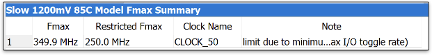 This is a screenshot of the Fmax Summary from the TimeQuest Timing Analyzer.
The Fmax column is what were interested in. Keep this value over 70MHz by breaking up large blobs of combinational logic with registers, and your design is guaranteed to work “as you coded it.” Let it fall below 70MHz, and all bets are off. HINT: trying to add 8x 16-bit values in a single clock cycle is probably not going to work :).
For this project, your system is required to meet the timing requirements of the 70MHz clock, as shown in that 1200mV, 85C model.
Timing Constraints
How did Quartus know that your clock was named CLOCK_50? Well, it has some hints from the inference process (i.e. it sees your always_ff blocks are posedge a signal that you connected to CLOCK_50).
If you want to tell Quartus what your clock is, then do the following:
Compile your design (just through elaboration is enough).
From the home screen, navigate to Tools ➙ Timing Analyzer along the top toolbar. You should see a window that looks like the following:
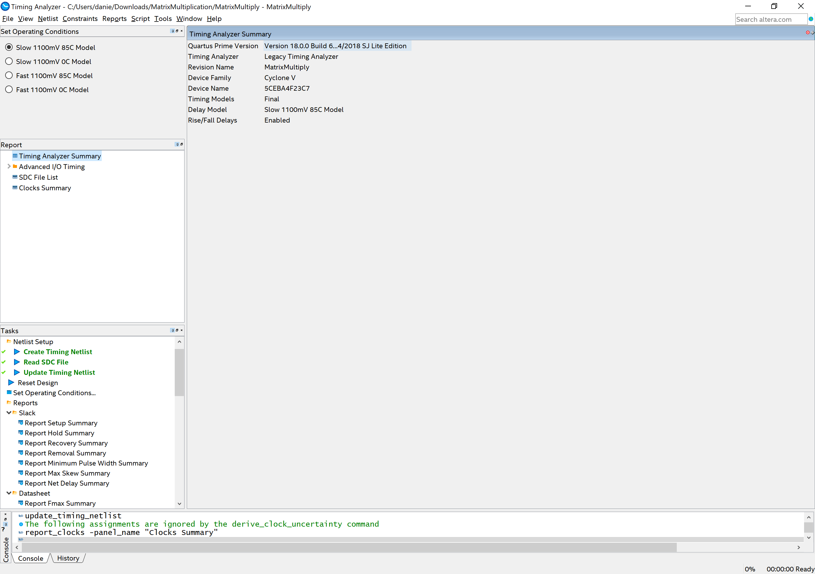 This is a screenshot of the Timing Analyzer window.
In the resulting window, use the taskbar on the bottom left to select Tasks ➙ Diagnostic ➙ Report Clocks. This will take a few seconds, but once it is complete the Timing Analyzer should generate a first-pass report for your design.
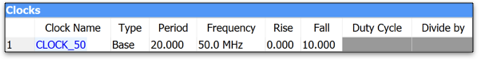
Under Clocks Summary you should see an entry for
CLOCK_50, but it might not have the correct constraints for Period, Rise, and Fall times. You can right-click the entries and select Edit Clock Constraint to fix the values. If yourCLOCK_50is not present, you can create it by going to Constraints ➙ Create Clock … along the top. Make sure the values match this exactly:
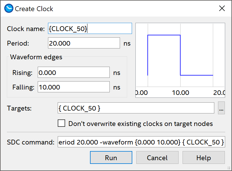 This is a screenshot of the Clock Constraints window.
Then, assuming everything looks good, go to Tasks ➙ Write SDC File … on the bottom-left to generate a constraints file. You may need to explicitly add this file to your Quartus project by going to Project ➙ Add/Remove Files in Project … and following the prompts like you would have for any new SystemVerilog file.
When you re-run the Timing Analyzer as part of the compilation flow in the future, it will have a listing for the clock you just created and constrained. It may give the same information as before, but now Quartus will be able to measure your critical paths accurate and decide if your design is feasible.
 This is a screenshot of the Timing Analyzer window showing the clock constraints.
For Credit
You will be graded on getting the right answer to the calculation, on the number of clock ticks it takes to do the calculation (smaller is better), if it meets timing, and your coding style.
The number of clock ticks? Yes, since the chip we have has lots of multiply units and block RAMs, you can organize the hardware and the A and B matrices (and copies of them) so that the calculations can run concurrently. You can use all of the hardware you want but the question is how fast can you make it run? You should count all clock ticks from when reset is no longer asserted and the calculation starts, until when the result of the calculation is stored in a register. After that, the clock tick counter doesn’t increment.
Getting the right answer? Note that you can organize your data in different ways to obtain fast implementations. You can apply some algebraic manipulations if you think it will be better. And remember, we’re only interested in the final summation of the Y vector. Actually, due to the limits on displays, we actually are only interested in the least significant 24-bits of the Y vector.
BTW, you must use the multiply and block RAM special features. I’m not sure why you wouldn’t, but I’ve heard reports of student is previous semesters trying to skip by without learning about the FPGA components. So sad for them…
Note that we will give a lot of points for just getting it to run. Getting it to run faster is worth more, see the grading sheet. 512 clock cycles is effectively your “speed of light” target, but don’t worry if your design is a bit slower. Do make sure you’re not truncating intermediate values though, otherwise you might be fast but inaccurate!
Model Organization
The header for your module should resemble the following:
module ChipInterface
  (input  logic       CLOCK_50,
   input  logic [9:0] SW,
   input  logic [3:0] KEY,
   output logic [6:0] HEX5, HEX4, HEX3, HEX2, HEX1, HEX0);
BUTTON0, when depressed, will reset the system.
Develop your code in a file called matrix_multiply.sv. There is really no TA testbench for this project. It just runs on the DE10 board and shows its results. To do the calculation again, hit reset (you should get the same result). That being said, feel free to make your own using the template file TB!
The ROMs and multiplier that you will instantiate are detailed below. The two matrices (ROMs) are initialized via the *.mif files. We are providing two different A, B, and C matrices. The A matrix is provided in contiguous row-major order.
matA_1.mif,matB_1.mif,matC_1.mifwill produce the result 24’h206D3D.matA_2.mif,matB_2.mif,matC_2.mifwill produce the result 24’h9409CF.
To use these, copy one set (e.g., all *_1.mif, or all *_2.mif) files to matA.mif, matB.mif, and matC.mif files and use the Makefile as specified below. The result given above is what you should expect to see if you’ve done the calculations correctly.
We have also provided a python script generate_matrix.py, which you can use to generate a random problem if you like (it even prints out the answer). We will be grading you with a random problem generated from this python program.
1
2
3
4
$ python generate_matrix.py matA_gen.mif matB_gen.mif matC_gen.mif

Matrix files created: matA_gem.mif matB_gen.mif matC_gen.mif
Accumulated product: 0x89779d
To make use of the Block RAM and embedded multipliers, instantiate, connect and use the according to the modules listed below. If you deviate too much from these, then the synthesis tool won’t recognize that you want the component and will do something else entirely.
Here are the headers of the component modules in a somewhat cleaned up format. We have provided these in romA_128x128.sv, romB_128x1.sv, romC_128x1.sv, and multiplier_8816.sv files. I wouldn’t recommend modifying those files, but feel free to look around inside.
module romA_128x128
 (input  logic [13:0] address_a, address_b,
  input  tri1         clock,  // I don't know why this is tri1
  output logic [7:0]  q_a, q_b);

// lots of generated code.  Don't touch!

endmodule : romA_128x128

module romB_128x1
  (input  logic [6:0] address_a, address_b,
   input  tri1        clock,  // Still no clue
   output logic [7:0] q_a, q_b);

... // lots of generated code.  Don't touch!

endmodule : romB_128x1

module romC_128x1
  (input  logic [6:0] address_a, address_b,
   input  tri1        clock,  // Still no clue
   output logic [15:0] q_a, q_b);

... // lots of generated code.  Don't touch!

endmodule : romC_128x1
romA_128x128 contains 16384 one-byte wide elements, hence the 14 bit address lines. romB_128x1 contains 128 one-byte wide elements, hence 7 bits for address lines. romC_128x1 contains 128 two-byte wide elements, hence 7 bits for address lines.
The ROMs are dual ported and thus you can provide two addresses and read two elements simultaneously. address_a address line provides the data read on q_a. The same is true for address_b and q_b.
The ROMs have registered inputs but unregistered outputs, meaning that the ROM loads the address values into its own internal registers at each clock edge. The results read from the ROM appear on q_a and q_b after that clock edge. So, you present the addresses in one state and read the results in the next.
The data in romA_128x128 is defined by romA.mif, romB_128x1 data is defined by romB.mif, and finally romC_128x1 data is defined by romC.mif. By specifying values for the ROM data, the on-chip implementation of the ROMs will be initialized to these values. See the note above about the two different sets of A, B, and C we have provided.
Hardware usage on the chip: romA_128x128 uses 16x M10K Embedded RAMs, romB_128x1 uses 1x M10K Embedded RAM, and romC_128x1 uses 1x M10K Embedded RAM. The Cyclone V chip has a total of 308 such block RAMs. Kudos if you can figure out why these are 10K memories instead of 9K (8192 bit) ones :).
The embedded multiplier has a module header that looks like:
module multiplier_8816
  (input  logic [7:0]  dataa, datab,
   output logic [15:0] result);

... // lots of generated code.  Don't touch!

endmodule : multiplier_8816
This is a byte multiplier that produces a 16-bit result. Simply connect the two operands into dataa and datab, and then patiently wait for the result to show up on result output combinationally.
Hardware usage on the chip: the above uses 1 9x9 multiplier. The 5CEBA4F23C7N Cyclone V chip has 198 such (independent) multipliers.
Simulating with QuestaSim
If you want to debug your design, you’re not going to have any fun sitting in the lab synthesizing and downloading again and again. The modules that tell Quartus to use the special hardware units (like the roms and multiplier) conveniently come with functional models that can be used in simulation. We’ve provided a simlib folder that include all of the Altera’s functional models .sv files in your directory.
To simulate, simply run the QuestaSim project with these file included and compile. In fact, the folder mds already included an example project.
QuestaSim may print some “Too few instance port connections” warnings from a file called altera_lnsim.sv. You can safely ignore these warnings.
Synthesizing with Quartus
If starting a new project, create a directory for the project. In this directory, place:
- romA_128x128.v
- romB_128x1.v
- romC_128x1.v
- multiplier_8816.v
- matA.mif
- matB.mif
- matC.mif
Start a project in Quartus with the Project Wizard. When prompted to add files to the project, add romA_128x128.v, romB_128x1.v, romC_128x1.v and multiplier_8816.v.
If a project already exists (like if you want to swap *.mif files), then in the Project Navigator window, switch to the Files tab. Right click on Files and click Add/Remove Files in Project.
Include a DE10_Standard_Pin_Assignment file to connect your pins.
Some Other Things you Should Learn
In the last project, I introduced you to the DE10 User Manual. That manual isn’t as useful for this project, as we are trying to use components that aren’t part of the board, but are part of the FPGA itself. Therefore, you should get to know a different manual — the Cyclone V Device Handbook. This manual is found on [https://intel.com] or on the DVD in the box (though the DVD has an earlier version, I haven’t found any issues with it). I have also posted a copy on BKeL. The manual describes, in great detail, everything that happens inside the FPGA. If you wanted to know how big the LUTs in the CLBs were, this is the document (chapter 2). If you wanted to know how the multipliers work (“hmm. I wonder if the multiplier can work on signed values?”) this is the document (chapter 5, in table 5-3). If you wanted to know how the memory blocks work (“hmm. I wonder if they support dual-port mode?”) this is the document (chapter 4, page 4-8).
Please take a few minutes to skim through the Cyclone V Device Handbook.
You should be using generate statements to instantiate (almost) all those embedded memories and multipliers. Because there will be a lot. A LOT.
How To Turn In Your Solution
This semester we will be using BKeL, simply submit the zip file with your reports and codes.
Demos and Late Penalty
We will have demo times outside of class times on or near the due date. Since we will demo from the files in your zip, it is possible that you’ll demo on a following day.
Define Late: Lateness is determined by the file dates of your submission on BKeL.